-


-
RFQ
 BOM Tool
 Manufacturer
-
 Help you save cost and time.
 -
 Provide reliable packaging for your goods.
 -
 Fast and reliable delivery to save time.
 -
 Excellent after-sales service.


International brand


Industrial parts

Blog
Part number
Popular parts
Latest parts
-
BCM52311A1HH0H275S
-
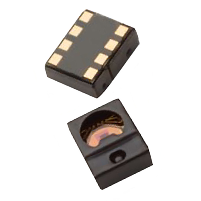
APDS-9160-003
-
APDS-9151
-
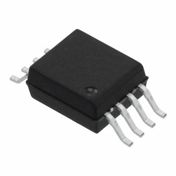
ACPL-C740-500E
-
ACPL-C740-000E
-
ACPL-0873-500E
-
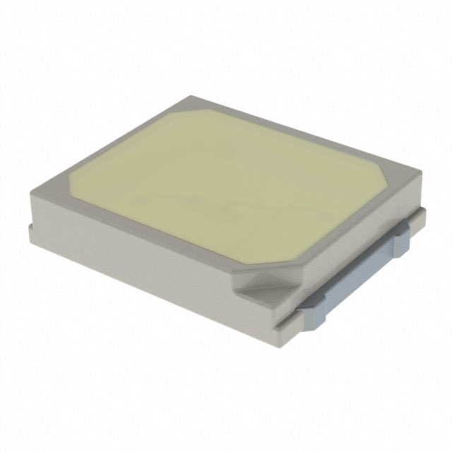
ASMW-LWG0-NEGFE
-
ASMW-LWG0-NEGDE
-
ASMW-LWG0-NEGBE
-
ASMW-LWG0-NDFHE
-
ASMW-LL00-NKM0E
-
ASMW-LD00-AGJ0E
-
ASMW-L300-AFH0E
-
ASMB-LTD2-0A333
-
ASMB-LTC2-0A335
-
VS-85HFL100S05
-
STA015$013TR
-
D225K100
-
SWT-1.02-168
-
VS-40HFL10S02
-
PDB-C615-2
-
RJS225E
-
Q4010NH5RP
-
TG80960JS33
-
STLC3055QTR
-
ST2042BD
-
NJM2711F-TE1
-
AD8612ARUZ
-
SN74ALVCH16374DL
-
TLV2470AIDR